Beyond lithography: Chinese chip toolmaker achieves wafer polishing breakthrough
Hwatsing Technology, a leading Chinese chip equipment maker, has announced a breakthrough in wafer polishing metrology for six-inch wafers, a critical step in semiconductor manufacturing.
Intelligence analysis by Gemini 2.5 Flash
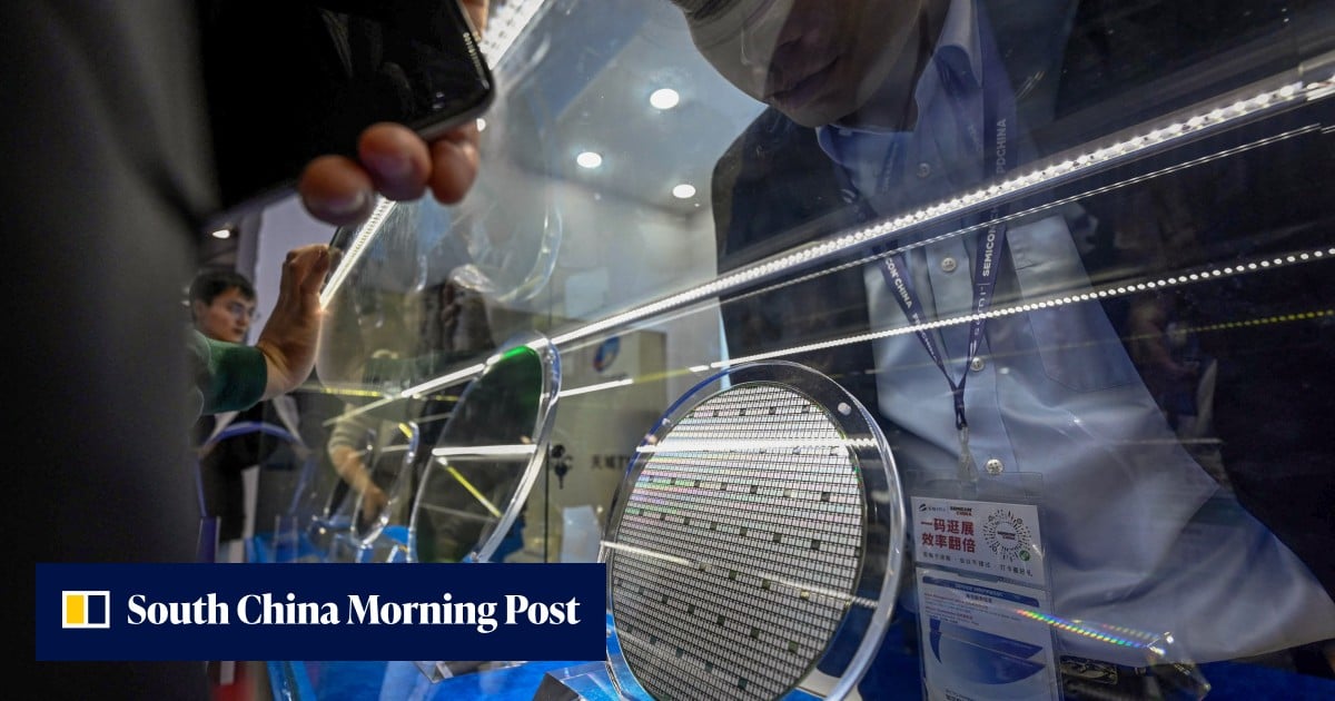
This development marks significant progress for China's domestic chip industry, as local equipment makers work to close the technology gap with foreign suppliers. The new system integrates real-time measurement into the polishing process, aiming to improve efficiency and reduce waste in chip production.
Imagine you're making a super tiny, super complicated LEGO castle. Before you can put all the tiny bricks together, you need a perfectly flat baseplate. This story is about a Chinese company that found a new way to make those baseplates, called 'wafers,' incredibly smooth and flat, like a perfectly ironed shirt. This helps make sure the tiny computer parts built on them work perfectly, making it easier for China to build its own advanced electronics.
Analysis
The recent announcement by Hwatsing Technology represents a notable advancement in China's efforts to bolster its domestic semiconductor manufacturing capabilities. While global attention often fixates on the most cutting-edge lithography processes, this breakthrough addresses a fundamental, yet equally critical, step in chip production: wafer polishing. This process is essential for creating the ultra-flat and smooth surfaces required for subsequent intricate layering and etching of microchips. The ability to perform this with high precision and integrated metrology is a testament to the incremental progress being made by Chinese firms in a highly complex global industry.
Hwatsing Technology
Hwatsing Technology, identified as China's leading producer of chemical mechanical polishing (CMP) equipment, is at the forefront of this development. The company's new metrology system is designed to identify defects and ensure manufacturing consistency, directly addressing a key challenge in semiconductor fabrication. By integrating this measurement tool directly into the polishing workflow, Hwatsing aims to provide real-time data feedback, which is critical for process control and optimization. This innovation underscores the strategic importance placed on domestic self-sufficiency in critical technology sectors within China.
Six-inch Wafers
The breakthrough specifically targets six-inch wafers, marking the country's first metrology system of this size to be paired with chemical mechanical polishing equipment. This focus on six-inch wafers, while not the most advanced in terms of size (larger wafers like 12-inch are common for leading-edge chips), is significant for certain types of integrated circuits and electronic devices. The direct integration of measurement before and after polishing is expected to enhance wafer uniformity and substantially reduce waste, thereby improving the overall efficiency of traditional production lines. This incremental but vital progress helps to solidify the foundation of China's semiconductor ecosystem.
Tianjin
Based in the northern city of Tianjin, Hwatsing Technology has already shipped its new system to an unnamed "leading domestic optical silicon materials producer." This indicates that the technology is moving beyond the research and development phase into practical application within China's industrial landscape. The deployment of such advanced domestic equipment is a strategic move to lessen reliance on foreign suppliers, particularly in the context of ongoing geopolitical tensions and technological restrictions. The success of this deployment will be a key indicator of China's ability to scale its indigenous chip manufacturing capabilities.
Key points
- Hwatsing Technology, a Chinese chip toolmaker, announced a breakthrough in wafer polishing metrology.
- The new system is designed for six-inch wafers and integrates real-time measurement into the polishing workflow.
- This direct integration aims to improve wafer uniformity and reduce waste in semiconductor manufacturing.
- The company has already shipped the new system to a domestic optical silicon materials producer.
- The development is part of China's broader effort to reduce dependence on foreign chip manufacturing technologies.
This breakthrough could significantly enhance China's domestic chip manufacturing capabilities, reducing its reliance on foreign technology and strengthening its supply chain resilience. Improved wafer polishing efficiency and quality could lead to more cost-effective and higher-performing chips for various applications, including AI.
Despite this progress, China remains heavily dependent on foreign suppliers for more complex and advanced chip manufacturing procedures, particularly in areas like lithography. This breakthrough, while important, addresses only one step in a multi-faceted process, indicating a long and challenging road ahead for achieving full technological self-sufficiency.