Peking University unveils 3D design tool to power Huawei’s chip ambitions
Peking University says it has built a prototype chip-design tool that works with Huawei's new LogicFolding architecture, aiming to support domestic semiconductor software.
Intelligence analysis by GPT-5.4 Mini
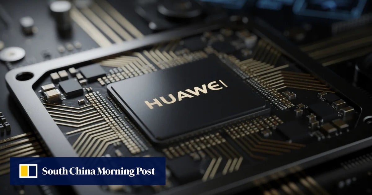
Peking University claims a prototype EDA tool that fits Huawei’s LogicFolding approach, part of a broader push to reduce reliance on Western chip-design software and tools under US export restrictions.
Peking University says it made a new computer program that helps people plan tiny computer chips before they are built. Think of it like a blueprint tool for a very small, very complicated city.
This matters because Huawei wants to make better chips, but some of the tools it used to depend on from other countries are harder to get now. A local tool could help it keep working.
The article says the new tool works with Huawei’s new chip plan. That is like making a puzzle piece that fits a new kind of puzzle board.
Analysis
What was announced
Peking University’s School of Integrated Circuits says researchers have unveiled a prototype electronic design automation (EDA) tool, software engineers use to design and test microchips before manufacturing. The university presents it as a domestic alternative in a market long dominated by Western firms such as Synopsys and Cadence Design Systems.
Why Huawei is in the picture
The tool is described as compatible with Huawei’s LogicFolding architecture, which Huawei introduced on Monday. That matters because Huawei is trying to keep advancing chip development despite US-led export controls that restrict access to key foreign tools and equipment. The article says Huawei wants chips by 2031 that can match the performance of advanced 1.4-nanometre technology without relying on Western chipmaking software subject to export bans.
The strategy shift
The story places this announcement inside a larger change in semiconductor strategy. For years, the industry improved performance mainly by shrinking transistors and packing more onto a wafer. After Washington blocked China’s access to advanced lithography machines needed for leading-edge production, Huawei shifted emphasis. Its new Tau (τ) Scaling Law, as described in the article, focuses on speed rather than smaller hardware: it tries to move electrical signals faster by lowering resistance and tightening internal wiring.
The article frames the Peking University tool as a supporting piece in that effort, not proof that China has solved the problem. It is a prototype, and the language in the report is careful: the university says it has made a breakthrough and says the tool is compatible with Huawei’s architecture. The larger implication is that domestic EDA software is becoming a strategic priority for Beijing as it tries to build a more self-sufficient chip stack.
Key points
- Peking University says it built a prototype EDA tool for chip design and testing.
- The tool is described as compatible with Huawei’s LogicFolding architecture.
- The report says domestic EDA is a priority because Western vendors dominate the market.
- Huawei is trying to advance chip design despite US export restrictions on key tools and equipment.
- The article links the effort to Huawei’s Tau Scaling Law, which focuses on speed rather than smaller transistors.